FPGA Releases: Difference between revisions
(K2 cores for the 2x are now available) |
|||
| (19 intermediate revisions by the same user not shown) | |||
| Line 1: | Line 1: | ||
# move the FG & BG Text LUT to: | |||
=== Important: === | === Important: === | ||
Most users will want to consume the "Firmware package relases" (taken from here: https://github.com/FoenixRetro/f256-firmware/releases. ) which contain both the latest of the FPGA releases seen here on this page, and the kernel/base programs intended for the flash memory. The page you're ready here is meant for power user who would want to test back compatibility or attempt some roll-backs in case bugs are found, and for readers who want to learn about the release notes of each new FPGA version. | Most users will want to consume the "Firmware package relases" (taken from here: https://github.com/FoenixRetro/f256-firmware/releases. ) which contain both the latest of the FPGA releases seen here on this page, and the kernel/base programs intended for the flash memory. The page you're ready here is meant for power user who would want to test back compatibility or attempt some roll-backs in case bugs are found, and for readers who want to learn about the release notes of each new FPGA version. | ||
''(* "Purple" refers to the official 2025+ release of the K2; "Black" refers to the first run of K2B boards sent out to the original F256K owners in late 2024)'' | ''(* "Purple" refers to the official 2025+ release of the K2; "Black" refers to the first run of K2B boards sent out to the original F256K owners in late 2024)'' | ||
=== Latest FPGA core files for all platforms === | |||
{| class="wikitable" | {| class="wikitable" | ||
! | ! colspan="3" | | ||
==== <big>F256Jr2</big> ==== | |||
! | |||
! colspan="3" | | |||
==== <big>F256K2</big> ==== | |||
|- | |- | ||
!Core | |||
!Link | |||
!Notes | |||
! | |||
!Core | |||
!Link | |||
!Notes | |||
|- | |- | ||
| | |6502 MMU | ||
|[https://github.com/Mu0n/F256MiscGoodies/blob/main/fpga/Jr2/Classic/2025-01-07/F256Jr2_MMU_Jan8th_2025_OPL3.mcs 08-Jan-2025] | |||
|OPL3 added | |||
! | |||
| | |6502 MMU | ||
| | |Black*: [https://github.com/Mu0n/F256MiscGoodies/blob/main/fpga/K2/CNTX1/2025-02-02/CFP95600C.bin 02-Feb-2025] | ||
| | Purple*: n/a | ||
|fix Onboard Access to a SPI Flash | |||
LCD Splash Screen | |||
|- | |- | ||
| | |65816 Ext | ||
| | |[https://github.com/Mu0n/F256MiscGoodies/blob/main/fpga/Jr2/Extended/2024-12-21/F256Jr2_Ext16_Dec21st_2024.mcs 21-Dec-2025] | ||
|Implementation of the 256Bytes | |||
Copy from Flash to RAM before booting. | |||
| | ! | ||
|[https://github.com/Mu0n/F256MiscGoodies/blob/main/fpga/K2/CNTX2/2025-01-07/CFP95616E.bin | |65816 Ext | ||
|Updated | |Black*: [https://github.com/Mu0n/F256MiscGoodies/blob/main/fpga/K2/CNTX2/2025-01-07/CFP95616E.bin 07-Jan-2025] | ||
Purple*: n/a | |||
|Updated access to WS6100 | |||
UART for the VS1053B | |||
|- | |- | ||
| | |65816 Ext 2x | ||
| | |[https://c256foenix.com/product-category/gen2-core/?v=5435c69ed3bc Buy Here] | ||
| | |2x CPU speed | ||
| | layer of 16 bit colored text | ||
| | |||
| | hardware line drawing | ||
64 more sprites. | |||
! | |||
|65816 Ext 2x | |||
|Black*: [https://github.com/Mu0n/F256MiscGoodies/raw/refs/heads/main/fpga/K2/CNTX4/F256K2x_Cores_Foenix138_BlackBoard_B3B_July27th_2025.bin 27-Jul-2025] | |||
Purple*: [https://github.com/Mu0n/F256MiscGoodies/raw/refs/heads/main/fpga/K2/CNTX4/F256K2x_Cores_Foenix138_B0C_August4th_2025.bin 4-Aug-2025] | |||
|2x CPU speed | |||
layer of 16 bit colored text | |||
hardware line drawing | |||
64 more sprites. | |||
! | |- | ||
! | |6809 | ||
|[https://github.com/Mu0n/F256MiscGoodies/raw/refs/heads/main/fpga/Jr2/6809/2025-06-15/F256JrJr_FNX6809_June14th_RC0014_0003.mcs 15-Jun-2025] | |||
|WIFI Speed and Interface (added TX_Empty & RX_Empty Flag) | |||
! | |||
|6809 | |||
|Black*: [https://github.com/Mu0n/F256MiscGoodies/raw/refs/heads/main/fpga/K2/CNTX3/NitrOS9_Load_BlackBoardB3B_WifiFixed_Sept4th.bin 04-Sep-2025] | |||
Purple*: [https://github.com/Mu0n/F256MiscGoodies/raw/refs/heads/main/fpga/K2Purple/CNTX3/NitrOS9_Load_PurpleBoardB0C_WifiFixed_Sept4th.bin 04-Sep-2025] | |||
|Wifi fix | |||
|- | |||
! colspan="3" | | |||
==== <big>F256Jr</big> ==== | |||
! | |||
! colspan="3" | | |||
==== <big>F256K</big> ==== | |||
|- | |||
!Core | |||
!Link | |||
!Notes | |||
! | |||
!Core | |||
!Link | |||
!Notes | |||
|- | |||
|6502 MMU | |||
|[https://github.com/Mu0n/F256MiscGoodies/blob/main/fpga/Jr/Classic/F256M_Wbh_Jan26th_2025_RC20_0100.jic 26-Jan-2025] | |||
|fixes Overlay FONT on top of graphic | |||
with Background Color Enabled | |||
! | |||
|6502 MMU | |||
|[https://github.com/Mu0n/F256MiscGoodies/blob/main/fpga/K/F256Kc_WBh_Jan26th_2025_RC16_0001.jic 26-Jan-2025] | |||
|fixes Overlay FONT on top of graphic | |||
with Background Color Enabled | |||
|- | |- | ||
| | |65816 Ext 2x | ||
| | |[https://github.com/Mu0n/F256MiscGoodies/raw/refs/heads/main/fpga/Jr/Extended/F256M_Wbh_Jun24th_2025_RC0100_0002.jic 24-Jun-2025] | ||
| | |Fixed bugs with register 0x0000 and 0x0001 | ||
! | |||
| | |65816 Ext 2x | ||
|[https://github.com/Mu0n/F256MiscGoodies/ | |[https://github.com/Mu0n/F256MiscGoodies/raw/refs/heads/main/fpga/K/F256Kc_WBh_Jun23th_RC0100_0003_DualSpeed_CPU.jic 23-Jun-2025] | ||
| | |Fixed bugs with register 0x0000 and 0x0001 | ||
|} | |} | ||
== F256Jr2 | === Previous FPGA core files for all platforms === | ||
Use these for testing out older softwares and snooping around for persistant issues. | |||
{| class="wikitable" | |||
|+ | |||
! colspan="3" | | |||
==== <big>Previous F256Jr2 Cores</big> ==== | |||
|- | |||
!Core | |||
!Link | |||
!Notes | |||
|- | |||
|6809 | |||
|[https://github.com/Mu0n/F256MiscGoodies/raw/refs/heads/main/fpga/Jr2/6809/2025-06-13/F256Jr2_FNX6809_June13th_RC0017_0002.mcs 13-Jun-2025] | |||
|Move the FG & BG Text LUT to: | |||
$18_3800 $18_383F TEXT_LUT_FG | |||
$18_3840 $18_387F TEXT_LUT_BG | |||
|- | |- | ||
| | |6809 | ||
|[https://github.com/Mu0n/F256MiscGoodies/raw/refs/heads/main/fpga/Jr2/6809/2025-06-11/F256Jr2_FNX6809_June11th_RC0017_0000.mcs 11-Jun-2025] | |||
|big Wishlist | |||
full access to write back the onboard flash | |||
| | |||
|- | |- | ||
| | |6809 | ||
|[https://github.com/Mu0n/F256MiscGoodies/blob/main/fpga/Jr2/6809/2025-01-17/F256Jr2_FNX6809_Jan17th_RC0014_0002.mcs 17-Jan-2025] | |||
|Fix for the manual Reset | |||
Fix for the readback of Multiplication Values | |||
|[https://github.com/Mu0n/F256MiscGoodies/blob/main/fpga/Jr2/ | |||
| | |||
Endianess | |||
Changes to: Line/Pixel Position | Changes to: Line/Pixel Position | ||
|} | |} | ||
=== Previous | {| class="wikitable" | ||
|+ | |||
! colspan="3" | | |||
==== <big>Previous</big> <big>F256K2</big> <big>Cores</big> ==== | |||
|- | |||
!Core | |||
!Link | |||
!Notes | |||
|- | |||
|6502 MMU | |||
|Black*: [https://github.com/Mu0n/F256MiscGoodies/blob/main/fpga/K2/CNTX1/2025-01-08/CFP95600C.bin 08-Jan-2025] | |||
Purple*: n/a | |||
|OPL3 implemented | |||
|- | |||
|6502 MMU | |||
|Black*: [https://github.com/Mu0n/F256MiscGoodies/blob/main/fpga/K2/CNTX1/2025-01-07/CFP95600C.bin 07-Jan-2025] | |||
Purple*: n/a | |||
|Instantiation of the UART for the VS1053B @ $DDB0 | |||
|- | |||
|6809 | |||
|Black*: [https://github.com/Mu0n/F256MiscGoodies/raw/refs/heads/main/fpga/K2/CNTX3/K2_NitrOS9_Load_BlackBoard_Aug26th.bin 26-Aug-2025] | |||
Purple*: [https://github.com/Mu0n/F256MiscGoodies/raw/refs/heads/main/fpga/K2Purple/CNTX3/FNX6809_First_Release_Aug24th_PurpleBoard.bin 24-Aug-2025] | |||
|This is the preliminary version and only works with a PS/2 keyboard plugged in. | |||
If destined for slot 3, rename the file and put in CNTX3/f256k2t9.bin | |||
|} | |||
{| class="wikitable" | {| class="wikitable" | ||
! | |+ | ||
! | ! colspan="3" | | ||
==== <big>Previous F256Jr Cores</big> ==== | |||
|- | |||
!Core | |||
!Link | |||
!Notes | |||
|- | |||
|6502 MMU | |||
|[https://github.com/Mu0n/F256MiscGoodies/blob/main/fpga/Jr/Classic/F256M_Wbh_Dec23rd_2023_RC18_0100.jic 23-Dec-2023] | |||
|Tiles fix; shifted by one towards the left. | |||
(0100 = Serial RAM/Flash Select) | |||
|- | |||
|6502 MMU | |||
|[https://github.com/Mu0n/F256MiscGoodies/blob/main/fpga/Jr/Classic/F256M_Wbh_Nov18th_2023_RC17_0100.jic 18-Nov-2023] | |||
|In light of decision to dump the big ticket items and the accessories from the store... | |||
* Removed the very SPI core introduced yesterday to drive the FNXNET51 module. | |||
* Removed the DP memory for the MMU and replace it back with simple Registers, which means that when you reset the system, the MMU, Page0 will be reset back to the way it was. However, the caveat is that if you change between RAM to FLASH MMU default value, you need to do a reset, either a debug reset or General Reset because the MMU is now only 32bytes in Size, so, 4 pages of 8 values. | |||
|- | |- | ||
| | |6502 MMU | ||
| | |[https://github.com/Mu0n/F256MiscGoodies/blob/main/fpga/Jr/Classic/F256M_WBh_Nov17th_2023_RC16_0111.jic 17-Nov-2023] | ||
| | | | ||
| | * No Write Allowed when Debug Port writes in the MMU Memory Zone | ||
| | * Incorporation of a new SPI Controller to interface with the FNXNET51 module using the NES/SNES MiniDin9 Connector | ||
* ReSync of the Debug Generated RDY to stop the CPU. (untested) | |||
|- | |||
|6502 MMU | |||
|[https://github.com/Mu0n/F256MiscGoodies/tree/main/fpga/Jr/Classic various older] | |||
| | | | ||
| | |- | ||
|65816 Ext 2x | |||
|[https://github.com/Mu0n/F256MiscGoodies/raw/refs/heads/main/fpga/Jr/Extended/F256M_Wbh_Jun17th_2025_RC0100_0001.jic 16-Jun-2025] | |||
|CPU runs at 2x speed at 12 MHz | |||
MUST use a 65816 cpu chip, | |||
will not work with the 6502 | |||
|- | |- | ||
| | |6809 | ||
| | |n/a | ||
|n/a | |||
| | |||
|} | |} | ||
{| class="wikitable" | {| class="wikitable" | ||
! | |+ | ||
! colspan="3" | | |||
==== <big>Previous</big> <big>F256K</big> <big>Cores</big> ==== | |||
|- | |- | ||
!Core | |||
!Link | |||
!Notes | |||
|- | |- | ||
| | |6502 MMU | ||
| | |[https://github.com/Mu0n/F256MiscGoodies/blob/main/fpga/K/2024-12-23/F256K_WBh_Dec23rd_RevB0x_RC14_0000.jic 23-Dec-2023] | ||
|Tiles fix; shifted by one towards the left. | |||
|- | |||
|6502 MMU | |||
[https:// | |[https://github.com/Mu0n/F256MiscGoodies/blob/main/fpga/K/F256K_WBh_Dec9th_RevB0x_RC13_0000.jic 09-Dec-2023] | ||
| | | | ||
* Fixes a problem with Interrupt from timer0 that was working on the Jr. | * Fixes a problem with Interrupt from timer0 that was working on the Jr. | ||
* Resolves a discrepancy between the F256Jr interrupt block and the F256K. | * Resolves a discrepancy between the F256Jr interrupt block and the F256K. | ||
|- | |- | ||
| | |6502 MMU | ||
|[https://github.com/Mu0n/F256MiscGoodies/blob/main/fpga/K/F256K_WBh_Nov19th_RevB0x_RC12_0011.jic 19-Nov-2023] | |||
| | |Corrects the issue with no-response from command $20 & $21 (not being processed in the early parser). The Jr doesn't have the issue. | ||
| | |||
Corrects the issue with no-response from command $20 & $21 (not being processed in the early parser). | |||
The Jr doesn't have the issue. | |||
|- | |- | ||
| | |6502 MMU | ||
|various older | |various older | ||
| | | | ||
| | |- | ||
| | |65816 Ext 2x | ||
| | |[https://github.com/Mu0n/F256MiscGoodies/raw/refs/heads/main/fpga/K/F256Kc_WBh_Jun18th_2025_RC0100_0000_DualSpeed_CPU.jic 18-Jun-2025] | ||
|CPU runs at 2x speed at 12 MHz | |||
MUST use a 65816 cpu chip, | |||
will not work with the 6502 | |||
|- | |||
|6809 | |||
|N/A yet | |||
|N/A yet | |||
|} | |} | ||
---old version will be kept at the bottom for a while in case errors are found above--- | |||
== FPGA Upgrade Guide == | == FPGA Upgrade Guide == | ||
| Line 264: | Line 286: | ||
|+ | |+ | ||
!Folder | !Folder | ||
! | !Hard coded file name | ||
!Typical* usage | |||
!CPU in the FPGA | !CPU in the FPGA | ||
|- | |- | ||
|CNTX1 | |CNTX1 | ||
|CFP95600C.bin | |||
|F256 Classic mode with a memory management unit (MMU), where the CPU sees 64k at once | |F256 Classic mode with a memory management unit (MMU), where the CPU sees 64k at once | ||
|65816 acting as 6502 | |65816 acting as 6502 | ||
|- | |- | ||
|CNTX2 | |CNTX2 | ||
|CFP95616E.bin | |||
|F256 Extended mode with a flat memory map all accessible at once | |F256 Extended mode with a flat memory map all accessible at once | ||
|65816 | |65816 | ||
|- | |- | ||
|CNTX3 | |CNTX3 | ||
|F256 with the 6809 core | |f256k2t9.bin | ||
|F256 with the 6809 core (planned) or 68000 core (planned) | |||
|6809 | |6809 | ||
|- | |- | ||
|CNTX4 | |CNTX4 | ||
| | |foenix138.bin | ||
|F256 with 2x CPU speed Extended mode with a flat memory map all accessible at once | |||
|65816 | |||
|} | |||
====== Note* on typical usage ====== | |||
As long as you keep the proper hard coded names tied to their folder names, you can slide any core to any slot. For example, if you want the 2x core to be in the CTNX2 folder, just rename it appropriately to CFP95616E.bin as you put it into CTNX2/. | |||
====== F256K2 core prep steps: ====== | |||
# Take care of placing the bin file in the FPGA load uSD card | |||
# Set the core selecting DIP switches at the back of the unit. Down (towards bottom of the unit) = 0, Up (towards the upper side of the unit) = 1. See below for all possibilities. | |||
# Power up the unit. If this is the first time you're using that core and you've never done step 4 for it, it's normal to not have a properly booted initial software (ie superbasic or otherwise) | |||
# Write the firmware to the content of the flash. Each of the 4 cores have their own 512kb of reserved flash space that are selected at the same time as the core itself from the uSD FPGA load card. Once they are written to, they are set for future usages as you switch between cores and won't require further flash writes, unless you're doing updates. | |||
====== Core selecting DIP switches in the back ====== | |||
{| class="wikitable" | |||
|+ | |||
!Core 1 | |||
!Core 2 | |||
!Core 3 | |||
!Core 4 | |||
|- | |||
| | |||
[[File:Core1.png|thumb]] | |||
| | |||
[[File:Core3.png|thumb]] | |||
| | | | ||
[[File:Core2.png|thumb]] | |||
| | |||
[[File:Core4.png|thumb]] | |||
|- | |||
|0 0 | |||
|1 0 | |||
|0 1 | |||
|1 1 | |||
|} | |} | ||
Latest revision as of 19:18, 16 December 2025
- move the FG & BG Text LUT to:
Important:
Most users will want to consume the "Firmware package relases" (taken from here: https://github.com/FoenixRetro/f256-firmware/releases. ) which contain both the latest of the FPGA releases seen here on this page, and the kernel/base programs intended for the flash memory. The page you're ready here is meant for power user who would want to test back compatibility or attempt some roll-backs in case bugs are found, and for readers who want to learn about the release notes of each new FPGA version.
(* "Purple" refers to the official 2025+ release of the K2; "Black" refers to the first run of K2B boards sent out to the original F256K owners in late 2024)
Latest FPGA core files for all platforms
F256Jr2 |
F256K2 | |||||
|---|---|---|---|---|---|---|
| Core | Link | Notes | Core | Link | Notes | |
| 6502 MMU | 08-Jan-2025 | OPL3 added | 6502 MMU | Black*: 02-Feb-2025
Purple*: n/a |
fix Onboard Access to a SPI Flash
LCD Splash Screen | |
| 65816 Ext | 21-Dec-2025 | Implementation of the 256Bytes
Copy from Flash to RAM before booting. |
65816 Ext | Black*: 07-Jan-2025
Purple*: n/a |
Updated access to WS6100
UART for the VS1053B | |
| 65816 Ext 2x | Buy Here | 2x CPU speed
layer of 16 bit colored text hardware line drawing 64 more sprites. |
65816 Ext 2x | Black*: 27-Jul-2025
Purple*: 4-Aug-2025 |
2x CPU speed
layer of 16 bit colored text hardware line drawing 64 more sprites. | |
| 6809 | 15-Jun-2025 | WIFI Speed and Interface (added TX_Empty & RX_Empty Flag) | 6809 | Black*: 04-Sep-2025
Purple*: 04-Sep-2025 |
Wifi fix | |
F256Jr |
F256K | |||||
| Core | Link | Notes | Core | Link | Notes | |
| 6502 MMU | 26-Jan-2025 | fixes Overlay FONT on top of graphic
with Background Color Enabled |
6502 MMU | 26-Jan-2025 | fixes Overlay FONT on top of graphic
with Background Color Enabled | |
| 65816 Ext 2x | 24-Jun-2025 | Fixed bugs with register 0x0000 and 0x0001 | 65816 Ext 2x | 23-Jun-2025 | Fixed bugs with register 0x0000 and 0x0001 | |
Previous FPGA core files for all platforms
Use these for testing out older softwares and snooping around for persistant issues.
Previous F256Jr2 Cores | ||
|---|---|---|
| Core | Link | Notes |
| 6809 | 13-Jun-2025 | Move the FG & BG Text LUT to:
$18_3800 $18_383F TEXT_LUT_FG $18_3840 $18_387F TEXT_LUT_BG |
| 6809 | 11-Jun-2025 | big Wishlist
full access to write back the onboard flash |
| 6809 | 17-Jan-2025 | Fix for the manual Reset
Fix for the readback of Multiplication Values Endianess Changes to: Line/Pixel Position |
Previous F256K2 Cores | ||
|---|---|---|
| Core | Link | Notes |
| 6502 MMU | Black*: 08-Jan-2025
Purple*: n/a |
OPL3 implemented |
| 6502 MMU | Black*: 07-Jan-2025
Purple*: n/a |
Instantiation of the UART for the VS1053B @ $DDB0 |
| 6809 | Black*: 26-Aug-2025
Purple*: 24-Aug-2025 |
This is the preliminary version and only works with a PS/2 keyboard plugged in.
If destined for slot 3, rename the file and put in CNTX3/f256k2t9.bin |
Previous F256Jr Cores | ||
|---|---|---|
| Core | Link | Notes |
| 6502 MMU | 23-Dec-2023 | Tiles fix; shifted by one towards the left.
(0100 = Serial RAM/Flash Select) |
| 6502 MMU | 18-Nov-2023 | In light of decision to dump the big ticket items and the accessories from the store...
|
| 6502 MMU | 17-Nov-2023 |
|
| 6502 MMU | various older | |
| 65816 Ext 2x | 16-Jun-2025 | CPU runs at 2x speed at 12 MHz
MUST use a 65816 cpu chip, will not work with the 6502 |
| 6809 | n/a | n/a |
Previous F256K Cores | ||
|---|---|---|
| Core | Link | Notes |
| 6502 MMU | 23-Dec-2023 | Tiles fix; shifted by one towards the left. |
| 6502 MMU | 09-Dec-2023 |
|
| 6502 MMU | 19-Nov-2023 | Corrects the issue with no-response from command $20 & $21 (not being processed in the early parser). The Jr doesn't have the issue. |
| 6502 MMU | various older | |
| 65816 Ext 2x | 18-Jun-2025 | CPU runs at 2x speed at 12 MHz
MUST use a 65816 cpu chip, will not work with the 6502 |
| 6809 | N/A yet | N/A yet |
---old version will be kept at the bottom for a while in case errors are found above---
FPGA Upgrade Guide
How to Upgrade the F256K FPGA (and F256Jr)
Note that the below Video Guide applies to both the F256K & F256Jr, despite it just being titled F256K.
You will need to download Quartus Prime Lite 18.1 Edition, since you are going to target a EP4CE15 FPGA (Cyclone 4).
Do not update to the latest version of Quartus Prime Lite, as the latest version doesn’t support that family of FPGA anymore and the software is very big.
Also, one might want to download only the "Intel® Quartus® Prime Programmer and Tools" as opposed to download the whole software by clicking on "Additional Software"
Intel Quartus Prime Lite Edition 18.1 for Windows
Intel Quartus Prime Lite Edition 18.1 for Linux
How to Upgrade the FPGA for the F256K2
It is possible that there will be more graceful methods in the future, but for now, the easiest is to pop off the uSD card found on the left side of the board marked "uSD Card / FPGA Load" and to replace the .bin files inside the directory of the root of that uSD card, using a modern computer.
This will of course imply that you open up your case. There is a guide on how to do so for the original F256K enclosure. Perhaps the F256K2 enclosure will be similar.
For those unfamiliar with the process of removing the uSD card from these slide-operation holders here is the process:
1) very gently press down on the middle metal locking slider that goes across on top of the uSD card and slide it towards the left.
2) the uSD card and its locking slider will now open up by rotating towards the left with a hinge on the left side
Inside the root of this uSD card, there are four folders marked as CNTX# where # is a number from 1 to 4. Simply replace the .bin file therein to update any one given core. You may completely ignore .prm files since they do not affect the F256K2.
| Folder | Hard coded file name | Typical* usage | CPU in the FPGA |
|---|---|---|---|
| CNTX1 | CFP95600C.bin | F256 Classic mode with a memory management unit (MMU), where the CPU sees 64k at once | 65816 acting as 6502 |
| CNTX2 | CFP95616E.bin | F256 Extended mode with a flat memory map all accessible at once | 65816 |
| CNTX3 | f256k2t9.bin | F256 with the 6809 core (planned) or 68000 core (planned) | 6809 |
| CNTX4 | foenix138.bin | F256 with 2x CPU speed Extended mode with a flat memory map all accessible at once | 65816 |
Note* on typical usage
As long as you keep the proper hard coded names tied to their folder names, you can slide any core to any slot. For example, if you want the 2x core to be in the CTNX2 folder, just rename it appropriately to CFP95616E.bin as you put it into CTNX2/.
F256K2 core prep steps:
- Take care of placing the bin file in the FPGA load uSD card
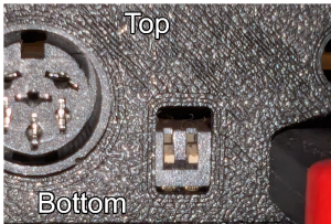
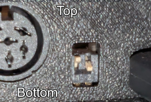
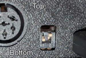
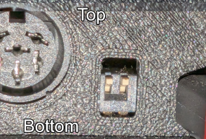
- Set the core selecting DIP switches at the back of the unit. Down (towards bottom of the unit) = 0, Up (towards the upper side of the unit) = 1. See below for all possibilities.
- Power up the unit. If this is the first time you're using that core and you've never done step 4 for it, it's normal to not have a properly booted initial software (ie superbasic or otherwise)
- Write the firmware to the content of the flash. Each of the 4 cores have their own 512kb of reserved flash space that are selected at the same time as the core itself from the uSD FPGA load card. Once they are written to, they are set for future usages as you switch between cores and won't require further flash writes, unless you're doing updates.
Core selecting DIP switches in the back
| Core 1 | Core 2 | Core 3 | Core 4 |
|---|---|---|---|
 |
 |
 |
 |
| 0 0 | 1 0 | 0 1 | 1 1 |
How to Upgrade the FPGA for the F256Jr. the 2nd
Go look at this guide here in the wiki.
Suggested USB Blaster (K and Jr. only)
Earth People Technology [1] [2]
Terasic USB Blaster (low cost version) [3] [4]
Chinese Knockoff (please avoid if possible)
Open Source blaster software (K and Jr. only)
For those who are struggling to program the FPGA with Linux or Apple, Stef found this great tool: