Hardware
Hardware Overview and Comparison
Special note on the K2 board revisions: the PCB color has 2 variants - "Purple" refers to the official 2025+ release of the K2; "Black" refers to the first run of K2B boards sent out to the original F256K owners in late 2024. The major change done to the purple board is that the Sii9022 is gone, so the HDMI encoding is done by the FPGA (like the JrJr), so the FPGA load is quite different.
|
F256Jr |
F256Jr the 2nd ("Jr.Jr.") |
F256K |
F256K2 | |
|---|---|---|---|---|
|
CPU |
WDC W65C02S |
onboard TQFP – WDC W65C816 CPU |
WDC W65C02S |
onboard TQFP – WDC W65C816 CPU |
|
RAM |
512 KB |
2MB SRAM (1Mx16) On Board (could be limited by Core) |
512 KB |
2MB SRAM (1Mx16) On Board (could be limited by Core) |
|
Flash |
512 KB |
512 KB |
512 KB |
512 KB Per Context (4x Contexts) |
|
FPGA |
Cyclone IV EP4CE15
15,408 Logic elements |
Artix 7 XC7A35T
33,280 Logic cells |
Cyclone IV EP4CE15
15,408 Logic elements |
Artix 7 XC7A200T
215,360 Logic cells |
|
Graphic Core |
TinyVicky |
TinyVicky II |
TinyVicky |
Vicky "The Fourth" |
|
Audio |
2 x PSG (FPGA Emulation) |
2 x PSG (FPGA Emulation) |
2 x PSG (FPGA Emulation) |
2 x PSG (FPGA Emulation) |
|
Connections |
1 x DVI (digital & analog) |
1 x Micro HDMI (Digital TMDS) |
1 x DVI (digital & analog) |
1 x HDMI (Digital TMDS) |
Hardware Details
CPU
The basic setup of all F256 is the Western Design Center 65C02, a slightly enhanced CMOS version of the very popular 6502 CPUs. The main difference to the 6502 in the 1970s and 1980s is the faster clock speed and the lower power consumption.
The 65C02 can also be replaced with a 65816 as a drop in replacement. Note, however, that while the 65c02 includes the additional Rockwell instructions (BBS/BBR, RMB/SMB), the 65816 does NOT. Therefore, these instructions should be avoided to ensure compatibility with F256 machines using the 65816.
In the F256, the CPU is always clocked at 6,29 MHz (6,293,750 Hz to be exact, derived from 25.175 MHz / 4 as discussed on Discord).
Frequencies for sound chips
The base frequency for which the various sound chips derive their own frequencies is based on the 14.31818 MHz NTSC M color subcarrier, used in various computing architectures, such as the PC ISA bus. The exact generating formula is 315/22 MHz.
The OPL3 chip uses 14.31818 MHz.
The PSG uses a divided by 4 value, hence 3.5795 MHz.
The SID uses a divided by 14 (NTSC version) value, therefore 1.022727 MHz.
Memory Expansion Slot
The memory expansion slot, located on the top right (above the keyboard), is intended primarily for Memory Expansion. It provides Address lines A0 - A17 (for addressing 256K), and active low Chip Select signal (CS_RAM) and Output Enable (OE) for the 256K Expansion address range $100000 - $13FFFF.
Foenix produce a 256K RAM Expansion cartridge, based on the CY7C1010DV33-10VXI, a high speed (10ns) 2Mbit (256K × 8) 3.3V Parallel Static RAM device.
The Expansion Slot itself, is based on a 36 pin PCI-Express x1 socket.
As the Expansion Slot also features pins for IRQ input, PHI2 clock output, and Reset (all signals which are unnecessary for a simple Memory interface), the Expansion Slot is also a candidate for other expansion purposes.
Utilizing the Expansion Slot (for your own purposes)
Warning: All signals on the Expansion Port are 3.3V logic level, therefore it is important that no voltage exceeding 3.3V is ever presented on any Expansion Port pin, or you risk damage to your F256!
If interfacing 5V TTL level devices to the Expansion Port, it is essential that level converters are used.
As an example, if directly interfacing to the Expansion Port pins with 5V logic, then you could use the SN74LVC8T245 bi-directional level translator, with the DIR input controlled by the Port's R/Wn signal (for the D0 - D7 bi-directional data bus), and the OEn input controlled by the Port's OEn signal. For the uni-directional Address and Control lines, the DIR input can be hardwired.
Note that the SN74LVC8T245 is designed so that the control pins (DIR and OE) are referenced to Vcca ('A' side voltage supplied). Therefore, a common practice would be to use side A for the internal (3.3V) side of the voltage translation, such that DIR and OE can be directly controlled by the Expansion Port's 3.3V level R/Wn and OEn pins. Side B (and Vccb) then being the 5V TTL level referenced (external facing) side.
As another example, if you were interfacing directly to a 3.3V peripheral chip (e.g. A W65C22 VIA powered by Vdd = 3.3V), but wanting to level translate to 5V TTL levels on the VIA's Port Pins, then an auto-direction level translator like the TI TXS010x series (TXS0108, TXS0104, TXS0101), might be more appropriate.
Note that on the TXS010x series the control pin (OE) is also referenced to Vcca ('A' side voltage supplied). With the TXS series, the 'A' side is actually limited to a 1.4V - 3.6V range, so is inherently the 3.3V internal side. Side 'B' is 1.65V - 5.5V, so is used for the external 5V TTL level referenced (external facing) side. So, if you're tying the active high OE pin of a TXS device (to permanently enable), it should be pulled to Vcca (not Vccb!).
Expansion Slot pin-out
|
Signal |
Side B |
Side A |
Signal |
|---|---|---|---|
|
A4 |
B1 |
A1 |
nRST |
|
A3 |
B2 |
A2 |
A5 |
|
A2 |
B3 |
A3 |
A6 |
|
A1 |
B4 |
A4 |
A7 |
|
A0 |
B5 |
A5 |
A8 |
|
CS_RAMn |
B6 |
A6 |
OEn |
|
D0 |
B7 |
A7 |
D7 |
|
D1 |
B8 |
A8 |
D6 |
|
3V3 |
B9 |
A9 |
GND |
|
GND |
B10 |
A10 |
3V3 |
|
D2 |
B11 |
A11 |
D5 |
|
Key Notch | |||
|
D3 |
B12 |
A12 |
D4 |
|
R/Wn |
B13 |
A13 |
A9 |
|
A17 |
B14 |
A14 |
A10 |
|
A16 |
B15 |
A15 |
A11 |
|
A15 |
B16 |
A16 |
A12 |
|
A14 |
B17 |
A17 |
IRQn |
|
A13 |
B18 |
A18 |
PHI2 |
Expansion Slot - Signal Descriptions
|
Signal |
Description |
|---|---|
|
A0 - A17 |
Address Bus output (for addressing $100000 - $13FFFF Expansion space) |
|
D0 - D7 |
Data Bus (bi-directional) |
|
RSTn |
Reset output (active low) |
|
CS_RAMn |
Chip Select output for Address Range $100000 - $13FFFF (active low) |
|
OEn |
Output Enable output for a Read from Address Range $100000 - $13FFFF (active low) |
|
3V3 |
3.3V Power output from the F256 (intended to power Expansion Interface only - Don't Exceed 500ma) |
|
GND |
Digital Ground reference |
|
R/Wn |
Read/Write ouput (Read = high / Write = low) |
|
IRQn |
Interrupt Request input - Internal pull-up and non-shared (compatible with open-drain or totem-pole driven) |
|
PHI2 |
Phase 2 - Clock Output |
PS/2 Wiring Diagram for F256Jr

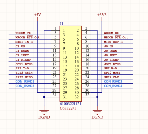
Header Pinout Diagram for F256JrJr
