FNX6809 Overview: Difference between revisions
(Initial page for FNX6809) |
m (→6809 core for the F256Jr2 & F256K2: better sized image) |
||
| (3 intermediate revisions by 3 users not shown) | |||
| Line 4: | Line 4: | ||
[[File:FNX6809_Adapter.jpeg|thumb|FNX6809 FPGA Flash Adapter]] | [[File:FNX6809_Adapter.jpeg|thumb|FNX6809 FPGA Flash Adapter]] | ||
The FNX6809 is a | The FNX6809 is a 40 pin dual inline package (DIP) module that is a cycle accurate implementation of the Motorola MC6809 CPU, working @ 3.3V and capable of running @ 6.29MHz on the F256Jr or the F256K. | ||
The FNX6809 also differs from a real Motorola MC6809 CPU in that it has the 65C02 pin-out. | The FNX6809 also differs from a real Motorola MC6809 CPU in that it has the 65C02 pin-out. | ||
| Line 10: | Line 10: | ||
For these reasons, it is not designed (at least for now) to be a direct replacement for an MC6809. | For these reasons, it is not designed (at least for now) to be a direct replacement for an MC6809. | ||
An | An adapter is supplied with the FNX6809 module to be enable reflashing the on-board FPGA, if ever needed. | ||
'''Note:''' | '''Note:''' | ||
* No software is written for the unit to support the processor at this time (but see [[OS-9]]). It is meant for | * No software is written for the unit to support the processor at this time (but see [[OS-9]]). It is meant for those Mavericks who are ready to take it on without any safety nets. There is a version of Calypsi that supports now if anybody wants to use it. | ||
* Keep in mind that you will need to upload a new load for the FPGA on the F256Jr or F256K to support it, so make sure you equip yourself with a USB Blaster. | * Keep in mind that you will need to upload a new load for the FPGA on the F256Jr or F256K to support it, so make sure you equip yourself with a USB Blaster. The loads can be found in the [[FPGA Releases]]. | ||
* There is a nice web-based 6809 emulator [http://6809.uk you can try here.] | |||
[[File:FNX6809_JTAG_Adapter_Position.jpg|thumb|left|FNX6809 JTAG Adapter Correct Orientation]] | |||
== 6809 core for the F256Jr2 & F256K2 == | |||
In the gen2, the 6809 exists within the big FPGA of both the Jr2 and K2. Only one load can exist at a time in the Jr2. For the K2, up to 4 loads can be copied over in separate folders called CNTX1, CNTX2, CNTX3 and CNTX4 inside the FPGA Load uSD card inside the case. The loads can be found in the [[FPGA Releases]]. | |||
=== Procedure to update the Jr2 for the 6809 load === | |||
to do | |||
=== Procedure to update the K2 for the 6809 load === | |||
(to improve with links?) | |||
You must verify which board color you own. The black boards were the first to be released in October 2024 as K2b in the Foenix store. The purple boards were sold a little later and is now the current revision of the K2. In both cases, | |||
* the fpga load that you get from [[FPGA Releases]] must be placed in the uSD card dedicated for FPGA loads, in the CNTX3 folder and the load itself must be renamed to f256k2t9.bin | |||
* Reinstall the SDCard | |||
* Set the DIP switch to position 3 like in the picture | |||
[[File:K2 dip3.png|thumb]] | |||
* Power on | |||
* write the FEU booter to the on-board flash memory (which occupies flash blocks 3d, 3e, 3f) | |||
* write the f0 core to the on-board flash memory | |||
* use a SD card with a goodies inside a .dsk file shared in the discord, it's possible to write it to a SD card using Balena Etcher under Windows | |||
Latest revision as of 14:44, 26 August 2025
FNX6809 for F256Jr & F256K


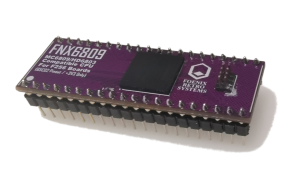
The FNX6809 is a 40 pin dual inline package (DIP) module that is a cycle accurate implementation of the Motorola MC6809 CPU, working @ 3.3V and capable of running @ 6.29MHz on the F256Jr or the F256K.
The FNX6809 also differs from a real Motorola MC6809 CPU in that it has the 65C02 pin-out.
For these reasons, it is not designed (at least for now) to be a direct replacement for an MC6809.
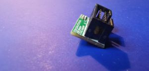
An adapter is supplied with the FNX6809 module to be enable reflashing the on-board FPGA, if ever needed.
Note:
- No software is written for the unit to support the processor at this time (but see OS-9). It is meant for those Mavericks who are ready to take it on without any safety nets. There is a version of Calypsi that supports now if anybody wants to use it.
- Keep in mind that you will need to upload a new load for the FPGA on the F256Jr or F256K to support it, so make sure you equip yourself with a USB Blaster. The loads can be found in the FPGA Releases.
- There is a nice web-based 6809 emulator you can try here.

6809 core for the F256Jr2 & F256K2
In the gen2, the 6809 exists within the big FPGA of both the Jr2 and K2. Only one load can exist at a time in the Jr2. For the K2, up to 4 loads can be copied over in separate folders called CNTX1, CNTX2, CNTX3 and CNTX4 inside the FPGA Load uSD card inside the case. The loads can be found in the FPGA Releases.
Procedure to update the Jr2 for the 6809 load
to do
Procedure to update the K2 for the 6809 load
(to improve with links?)
You must verify which board color you own. The black boards were the first to be released in October 2024 as K2b in the Foenix store. The purple boards were sold a little later and is now the current revision of the K2. In both cases,
- the fpga load that you get from FPGA Releases must be placed in the uSD card dedicated for FPGA loads, in the CNTX3 folder and the load itself must be renamed to f256k2t9.bin
- Reinstall the SDCard
- Set the DIP switch to position 3 like in the picture

- Power on
- write the FEU booter to the on-board flash memory (which occupies flash blocks 3d, 3e, 3f)
- write the f0 core to the on-board flash memory
- use a SD card with a goodies inside a .dsk file shared in the discord, it's possible to write it to a SD card using Balena Etcher under Windows